for an Invited Paper for the MAR12 Meeting of the American Physical Society Electrical characterization of interfacial defects GENNADI BERSUKER, SEMATECH Aggressive transistor scaling to achieve better chip functionality calls for the... more
We have modeled diffusion of H in a two-step Si 3 N 4 passivation process invoking the concept of "storage" of H. The H stored during nitridation is redistributed during a subsequent anneal. The modeling results agree with this... more
Nanomaterial, dengan ukuran dalam rentang nanometer, telah menarik perhatian luas dalam beberapa dekade terakhir karena sifat-sifatnya yang unik dan potensial untuk aplikasi yang luas. Salah satu aspek penting dari nanomaterial adalah... more
In photonic crystals made of materials with a frequency dependent dielectric function surface plasmon modes are extending over some adjacent layers and it turns out, that the dispersion can be tailored by coupling surface plasmons of... more
Crystallinity, optical band gap, resistivity and photoresponse of thermally evaporated In 2 S 3 thin films deposited at a temperature of 350 • C and further annealed in sulfur vapour at different temperature range of 200-300 • C is... more
Tin sulfoselenide (SnS 1-x Se x ) is a novel ternary semiconductor that belongs to the IV -VI group of compounds. It possesses the properties of both SnS and SnSe, which are proved as good absorber materials for solar cell fabrication. In... more
The structural, compositional, morphological and optical properties of In 2 S 3 thin films, prepared by thermal evaporation technique and annealed in sulfur ambient at different temperatures have been investigated. The grazing incident... more
Indium sulfide (In2S3) is a wide bandgap semiconductor, which is widely used as a window/buffer layer in thin film solar cell applications. In2S3 thin films were deposited using thermal evaporation technique and were annealed in sulfur... more
In this paper, we study the process of growth from the melt by Chokhralsky method of bulk β-Ga2O3 crystals. The effect of different configurations of growth zones and ambient composition on resulting bulk crystal quality has been... more
The article presents the results of the study of the mechanical properties and defect structure of gallium oxide (Ga2O3) by using the piezoelectric composite oscillator technique. Bulk samples of the Ga2O3 beta phase in the form of single... more
Results of successful experiments on the growth of gallium oxide (β-Ga 2 O 3) crystals by the Czochralski method are reported. The influence of growth atmosphere on the crystalline perfection of obtained material has been studied. It... more
The aluminum distribution in the surface layer of an (Al x Ga 1-x) 2 O 3 crystal grown on a sapphire seed by the Czochralski method has been studied using X-ray fluorescence and X-ray diffraction mapping and scanning electron microscopy.... more
A method is proposed for increasing the radiation resistance of semiconductor crystals (Al x Ga 1-x) 2 O 3 , which are promising for creating power electronics and optoelectronic devices for spacecraft performing tasks in near-earth... more
Bulk β-Ga 2 O 3 samples grown by the Czochralski method are studied. Based on the studies of the absorbed current dynamics and the cathodoluminescence, it is shown that there is a localization of charges of both signs in the sample. The... more
The present work is focussed on Zinc (2, 4, 6, 8 and 10 wt%) doped CdS thin films synthesized by sol-gel spin coating method and deposited on glass substrates. X-ray diffraction patterns of Zn doped CdS thin films exhibit cubic structure.... more
It is known that the thermal efficiency of materials is directly proportional to the product of the electrical conductivity multiplied by the thermo-electromotive force squared and inversely proportional to the thermal conductivity. To... more
The self-heating effect of the silicon-on-insulator (SOI)-raised-buried-oxide (RBOX) ferroelectric tunnel field effect transistor is explored in this article. Proposed device reliability issues have been examined by activating the... more
Here, the proposed device is a negative capacitance based ferroelectric gate stack, raised buried oxide pocket doped SOI TFET (RBOX-SOI-Fe TFET). The architecture of the device is carefully designed with proper optimization of the pocket... more
Zinc-cobalt sulphide (Zn x Co 1Àx S) thin films were fabricated on glass substrates using the chemical bath deposition (CBD) technique. In this study, the films were grown employing solutions of zinc acetate, cobalt sulphate, and... more
The public reporting burden for this collection of information is estimated to average 1 hour per response, including the time for reviewing instructions, searching existing data sources, gathering and maintaining the data needed, and... more
The public reporting burden for this collection of information is estimated to average 1 hour per response, including the time for reviewing instructions, searching existing data sources, gathering and maintaining the data needed, and... more
Gallium nitride pin rectifiers grown on bulk GaN substrate have been fabricated and characterised. The device structures were grown by metal organic chemical vapour deposition (MOCVD) on free-standing GaN substrates. The diode structure... more
An approach using a differential evolution (DE) optimization algorithm is proposed to optimize design parameters for improving the optical absorption efficiency of plasmonic solar cells (PSC). This approach is based on formulating the... more
The integration of AI and machine learning in precision mechanical systems has significantly transformed semiconductor lithography, enabling higher accuracy, enhanced system reliability, and optimized operational efficiency. This study... more
Electronic structure and vibrational characteristics of GaAlN wurtzoids at the molecular-nanoscale limit are investigated. The investigated properties include energy gap, vibrational properties, and phase stability against transition to... more
This research aims to study the growth of TiO2 under a direct imposition of a strong permanent neodymium magnet with a magnetic dipole. The objective of the research is to study the effect of the magnetic field imposition on the growth... more
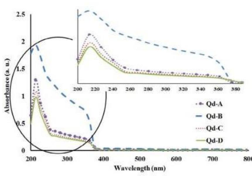
Quantum dot-sensitised solar cells (QDSSCs) have turned out to be strong alternatives in comparison to conventional solar cell technology, with important advantages like reduced environmental impact and cost. QDSSCs generate more... more


Traditionally, digital imaging systems rely on the use of dedicated photodetectors to capture specific wavelengths in the visible spectrum. These photodetectors, which are commonly made of silicon, are arranged as arrays to capture the... more
Optical and light emitting diode structures with an active InGaN region containing short period InGaN/GaN superlattices are studied. It is shown that short period superlattices are thin two dimensional layers with a relatively low In... more
We report on the electrical properties of the AlN/4H-SiC interface using capacitance-and conductance-voltage (CV and GV) analysis of AlN/SiC MIS capacitors. The crystalline AlN layers are made by hot wall MOCVD. CV analysis at room... more
We have calculated the plasmon frequency of the two-dimensional electron gas (2DEG) in AlGaN/GaN high electron mobility transistors (HEMT). The impact of HEMT's parameters on the plasmon frequency and the sheet charge density of the... more
In evaluating GaN HEMTs for high-power applications, it is crucial to consider the device-level breakdown characteristics. This work replaces the conventional AlGaN barrier and common AlGaN backbarrier with unstrained AlN, and it assesses... more
Epitaxy is a process by which a thin layer of one crystal is deposited in an ordered fashion onto a substrate crystal. The direct epitaxial growth of semiconductor heterostructures on top of crystalline superconductors has proved... more
Undoped AlN/GaN heterostructures, grown on sapphire by molecular beam epitaxy, exhibit very low sheet resistances, ~ 150 Ohm/sq, resulting from the 2-dimensional electron gas situated underneath a 4 nm thin AlN barrier. This... more
Presence and origin of interface charges at atomic-layer deposited Al2O3/III-nitride heterojunctions
Unlike silicon and traditional III-V semiconductors, the III-nitrides exhibit high spontaneous and piezoelectric polarization charges at epitaxial polar heterojunctions. In the process of investigating scaling properties of gate-stacks... more
Mn ions in (Ga,Mn)N exhibit a tendency to form pairs, which is enhanced by ferromagnetic Mn–Mn coupling. We also find that segregation of Mn to form MnN clusters in the wurtzite structure of host GaN is energetically favorable. However,... more
CdTe buffer layers which were grown on (211)B GaAs by molecular beam epitaxy were subjected to two different etch treatments to quantify the crystal quality and dislocation density. The optical properties and thicknesses of the samples... more
Аннотация. Последние разработки в области физики высокоиндексных резонансных диэлектрических наноструктур предлагают альтернативные механизмы управления субволновым светом, обусловленные резонансами Ми с сильным магнитным откликом,... more
A method for determining the band gap value and the refractive index near the absorption edge from reflection spectra was tested for CdS x Se 1-x films prepared using the screen-printing and sintering technique. Keywords: semiconductors,... more
I learned pretty early in life that you don't have to learn everything to be able to do something. With inventing, you are attempting to solve a problem within your reach, not trying to resolve the world's greatest problems. -Nick... more
In this work photoacoustic conversion efficiency was analyzed in the porous silicon (PSi) and in the composite based on it, such as the "porous matrix-liquid" was analyzed. The minimum of phase on frequency dependence was observed... more
Gated transmission line model pattern measurements of the transient current–voltage characteristics of AlGaN/GaN heterostructure field-effect transistors (HFETs) and metal–oxide–semiconductor HFETs were made to develop a phenomenological... more
The mechanism of radio-frequency current collapse in GaN–AlGaN heterojunction field-effect transistors (HFETs) was investigated using a comparative study of HFET and metal–oxide–semiconductor HFET current–voltage (I–V) and transfer... more
Bird Goën & Co. Klein Dalenstraat 42A 3020 Winksele (BE) (54) Improved cleaning of plasma chamber walls by adding of noble gas cleaning step (57) An improved reaction chamber and chamber cleaning process are disclosed able to remove water... more


