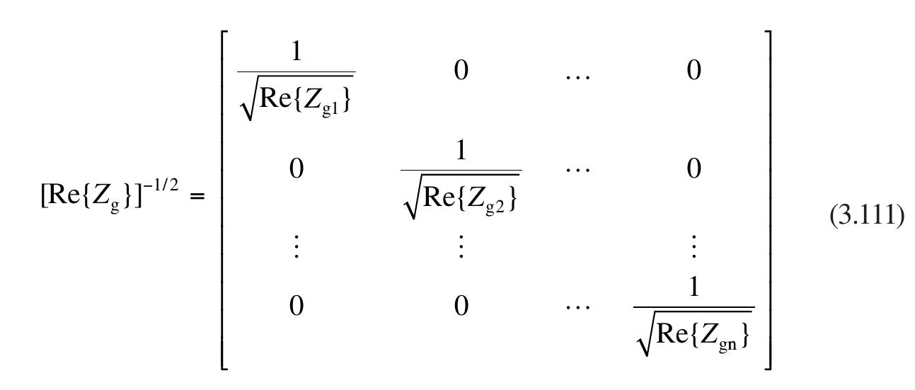
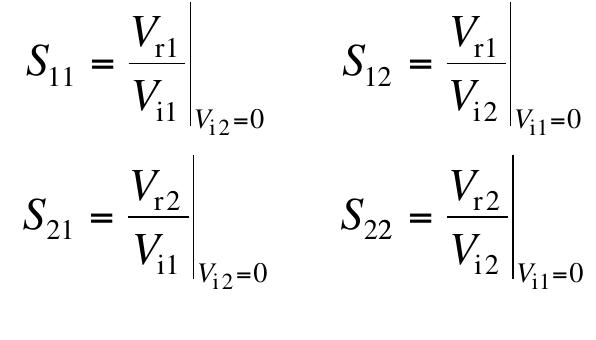
 Friend Name
Abstract
AI
AI
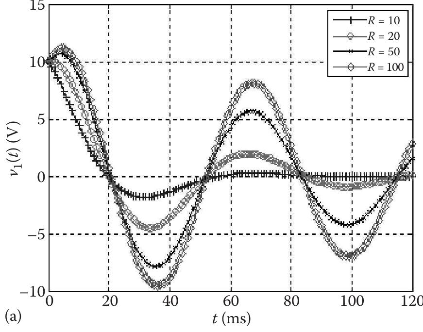
The paper discusses RF power amplifiers, covering their operational frequency ranges and the various classes of amplifier topologies, including linear and nonlinear amplifications. It highlights the characteristics and applications of different amplifier classes (A, B, AB, C, D, E, F, and S) and emphasizes the importance of switching-mode amplifiers in achieving efficient signal amplification across a wide frequency spectrum.
Figures (492)


![The nested sweep setup is When simulation is run, the I-V characteristics are obtained from the Probe interface. As seen from simulation results shown in Figure 2.12, V,,> V,,= 4.54 [V] as specified in the lib file that MOSFET conducts.](https://figures.academia-assets.com/56826516/figure_078.jpg)


![column titled “B” in Table 3.6. The measured S$ parameters were then plotted wit the vendor-supplied spice model under the same biasing conditions, as well as th catalog vendor data for the given biases. These results are detailed in Figures 3.5 through 3.54 when V., = 1O[V] and J, = 5[{mA]. As detailed in the S parameter plots the data measured using the BFR92 test fixture aligned themselves closely with bot the vendor-supplied spice model and the vendor catalog data. The comparison of th measured and simulated data has also been done for all other conditions shown i Table 3.6. The agreement again was seen on all of them.](https://figures.academia-assets.com/56826516/table_010.jpg)


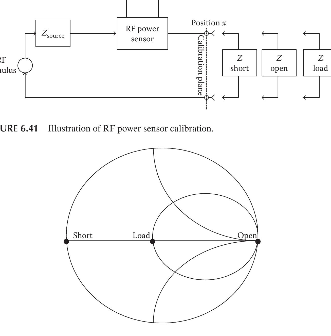
![EEE In this section, the analysis of multistate reflectometers based on a four-port network and a variable attenuator proposed in Ref. [42] and shown in Figure 6.36 is extended to examine the more general theory of using scalar power measure- ments to determine the complex reflection coefficient. The explicit closed-form relations and solutions for the system of equations are derived and used to calculate](https://figures.academia-assets.com/56826516/figure_378.jpg)


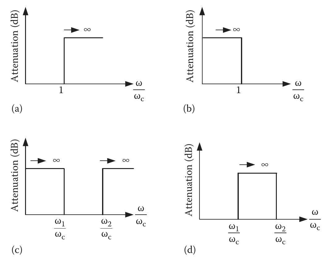
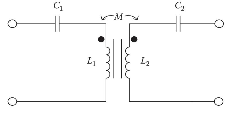
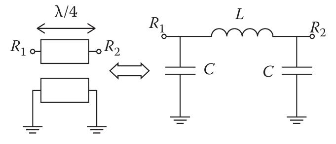
![ude ripples 1n the passband. Elliptic filters have steeper transition from passband to stopband similar Chebyshev filters and exhibit equal amplitude ripples in the passband and stopbat 2F/microwave filters and filter components can be represented using a two-pi 1etwork shown in Figure 7.3. The network analysis can be conducted using ABC yarameters for each filter. The filter elements can be considered as cascaded comfy 1ents, and hence, the overall ABCD parameter of the network is just a simple mat nultiplication of the ABCD parameter for each element. The characteristics of t ilter in practice are determined via insertion loss, S,,, and return loss, S,,. ABC yarameters can be converted to scattering parameters, and insertion loss and retu oss for the filter can be determined. The detailed analysis procedure for filters | een given in Ref. [1].](https://figures.academia-assets.com/56826516/figure_388.jpg)


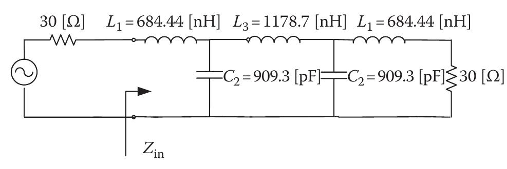
![The attenuation curves are obtained and given for several ripple values using MATLAB in Ref. [1] with examples. Example—F/2 LPF Design for RF Power Amplifiers Design an F/2 filter for an RF power amplifier that is operating at 13.56 MHz. The filter should have no impact during the normal operation of the amplifier. It should have at least 20-dB attenuation at F/2 frequency. The passband ripple should not exceed 0.1-dB ripple. It is given that the amplifier is presenting 30-Q impedance to load line. Solution](https://figures.academia-assets.com/56826516/figure_395.jpg)


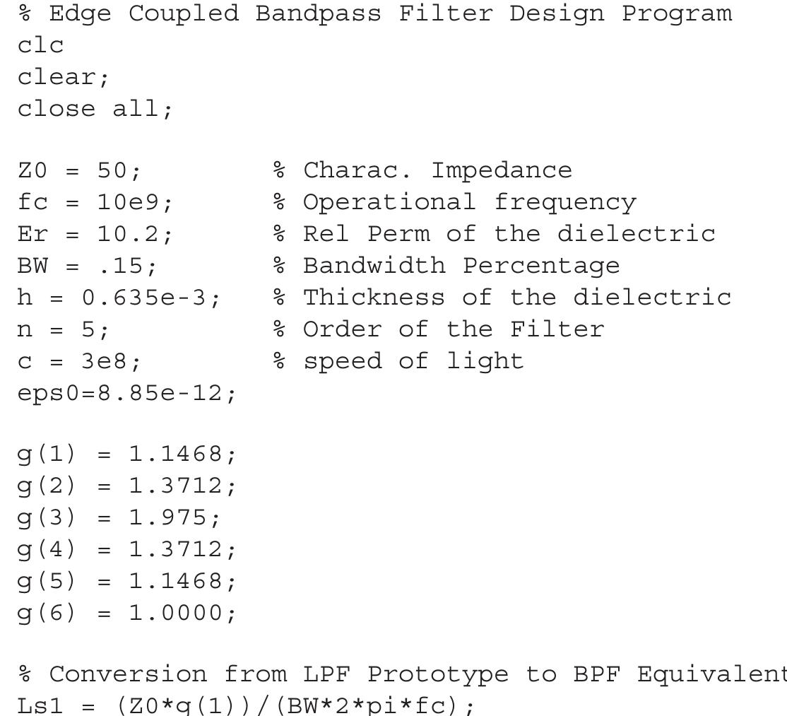
![These even- and odd-mode impedances are directly used to find the dimensions of the microstrips in the BPF. After the even- and odd-mode impedances are deter- mined, the synthesis technique introduced in Refs. [1,2] and in Chapter 6 is used to determine accurate physical dimensions. Based on the synthesis method, the spacing ratio between coupled lines is found using coupled microstrip lines. These values are also calculated in the MATLAB script from the following equations:](https://figures.academia-assets.com/56826516/figure_417.jpg)


![AMD is the arithmetic mean distance, and GMD is used for the geometric dis- tance. C is the capacitance that includes the effect of odd mode, even mode, and interline coupling capacitances between coupled lines of the spiral inductor. The detailed calculation of the capacitances is given in Ref. [9]. The substrate losses and conductor losses are ignored due to the low operational frequency. The one-port measurement network for the spiral inductor using the model pro-](https://figures.academia-assets.com/56826516/figure_447.jpg)


